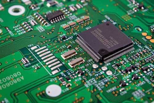
Here is a look at the process of PCB manufacturing or Printed Circuit Boards. The steps outlined below apply to most custom electronic designs.
Step one
Setting up the process which includes choosing processes, materials, and how to meet custom circuit board customers' specific needs for the design of the board.
Step Two
This is the imaging stage where the data is transferred onto etch resist film that then gets put on the copper conductive layer.
Step Three
Now is the time for the process of etching. The traditional method would expose the unprotected areas and the copper to a chemical leaving behind just the protected copper pads. More modern methods in this process of making a custom circuit board use lasers or plasma etching rather than chemicals as they give a better definition of the lines.
Step Four
Aligning the insulating dielectric layers and conductive copper under heat which are then pressed to turn the board into a solid material.
Step Five
Drilling holes for plated through applications. The second drilling for holes that are not going to have plating happens in step seven.
Step Six
Applying copper plating to the traces and the pads and holes. A bath of copper that is electrically charged holds the boards.
Step Seven
Now is the time for the second drilling of holes through an area of copper that is not going to be plated through. This does add extra cost to the process of custom electronic design boards.
Step Eight
Now is the time for the process of masking. Apply a material over the traces of bare copper and where there are thin amounts of solder over copper too. This protects them from damage and gives them better insulation and less likely to have problems with solder shorts.
Step Nine
At this stage of finishing it is time to apply a coating to the pad areas along with a fine layer of solder. This gets it ready for the reflow soldering or wave soldering that comes later once the components are in place.
Step Ten
Silk screening time which you can apply to both sides if both sides will have components or just the top side. The markings that designate components and the outlines of those components are applied.
Step Eleven
The routing step is where the separation of multiple boards occurs, and slots or notches are cut into them should that be a requirement.
Step Twelve
The boards need to have a visual inspection and checked for quality.
Step Thirteen
Time to test them. With electrical testing, the boards are checked for shorted connections by applying a volt to different points and making sure there is a flow of current. Some more complex boards need test programs and fixtures specifically designed to test them.


Leave a Comment